Nanotechnology Enables Printed Electrical Circuits Made from Wood
How nanotechnology can use wood to create ecologically sustainable circuit boards for the electronics industry.

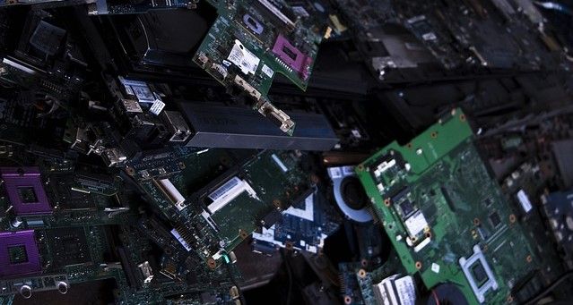
In today's world of electronics, where everything is fast and innovation is paramount, the production of circuit boards has become a business that is high-paced, high-cost, and often high-waste.
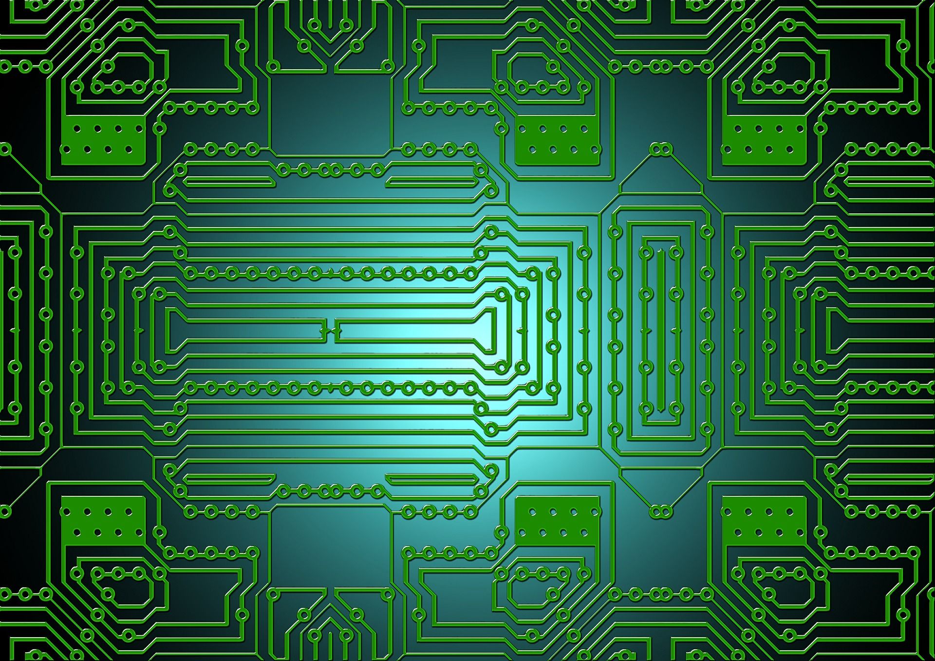
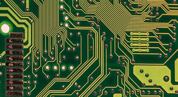
Printed circuit boards (PCBs) are the backbone of modern electronics and are found in almost every electronic device, from smartphones and computers to home appliances and cars. However, their production is not without its challenges, particularly in terms of sustainability.
PCBs are typically made from glass fibres soaked in epoxy resin, which makes them difficult to recycle and dispose of properly. This has prompted researchers from all over the world to look for alternative, more sustainable materials to use in the production of PCBs.
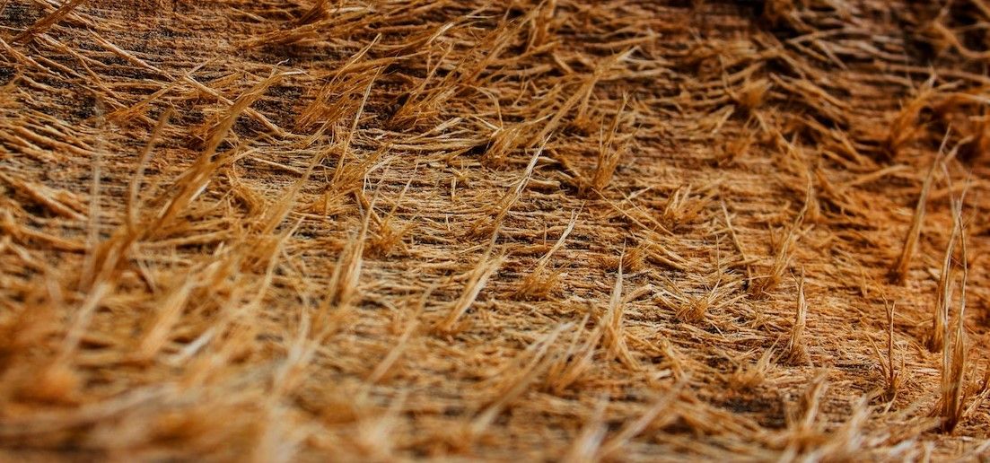
One such researcher is Thomas Geiger from Empa, the Swiss Federal Laboratories for Materials Science and Technology. Geiger has been researching tiny cellulose particles which measure as little as fifty nanometres wide (0.00005mm). Called fibrils, these nanomaterial fibres can be produced from wood pulp, agricultural waste, and other sources. Cellulose nanomaterials hold enormous potential for sustainable production and the decarbonization of industry since they grow CO2-neutral in nature, burn without residues, and are even compostable.
Geiger's work has led him to inquire if cellulose fibrils can be used to make biodegradable circuit boards that can reduce the ecological footprint of electronics.
Nanomaterials make Smaller, Eco-Friendly Printed Circuit Boards
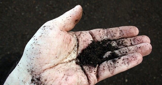
When mixed with water, the bio-fibrils produce a thick sludge that can be dewatered and compacted in a special press. Together with a colleague, he produced twenty experimental boards, which were subjected to various mechanical tests and finally fitted with electronic components.
The tests were successful, and the cellulose board released the soldered-on components after a few weeks in natural soil.
Geiger explains, “Cellulose fibers can be a very good alternative to glass fiber composites. We dewater the material in a special press with 150 tons of pressure. Then the cellulose fibrils stick together on their own without any additives. We call this ‘hornification’.”
Geiger’s lab has already developed various printed electronic components from biodegradable materials, such as batteries. Another Empa team, led by Gustav Nyström, built a biodegradable display based on hydroxypropyl cellulose (HPC), whereby adding a small amount of carbon nanotubes, the cellulose became electrically conductive.
The display changes colour depending on the applied electrical voltage and can also serve as a pressure or tension sensor and has the potential to play a role as a biodegradable user interface in future eco-electronics.

Nanomaterials for Next-Generation Circuitry
To overcome the limitations of traditional top-down manufacturing approaches, nanotechnology has played a significant role in advancing the design and production of PCBs. Advanced top-down nanofabrication techniques enable smaller overall size and patterns on the PCB surfaces.
However, even these methods have their limitations. As such, nanotechnology has also brought forth bottom-up approaches to build circuit boards atom by atom, creating circuit boards that are much smaller than what could be achieved through top-down fabrication. The ability to build atomic structures and devices in this way is a valuable tool in ushering in smaller and more advanced PCBs that require more complex circuitry.
Moreover, nanotechnology has revolutionized component integration on the PCBs by reducing component size while improving performance - transistors are a prime example. Many nanomaterial-inspired transistors have been integrated into PCBs, offering enhanced performance and smaller sizes, leading to better speed, power, and overall capabilities of the PCB.
Nanomaterials in Printed Circuit Boards Coatings
Nanomaterials have already made an impact on the electronics manufacturing sector when employed in coatings that protect PCBs against environmental factors such as impact, abrasion, and water/moisture. Alternatively, they can be used to dissipate localized heat spots that can arise within a device. These properties are especially useful for electronic circuits used in remote, environmental, and chemical process monitoring environments.
Some nanocoatings can also enhance the conductivity of the PCB and components attached to it - known as conductive coatings. Nanomaterials, therefore, prove useful in enhancing the properties of PCBs without the need for direct integration into the PCB itself.
Though electronic coatings have been used for many years, utilizing nanomaterials as the active component of these coatings offers several advantages. For example, nanocoatings are significantly thinner, conform better to complex surface geometries, and possess nano-level uniformity.
Nanomaterials for Sustainable Circuit Boards
However, the breakthrough for ecologically sound and sustainable electrical circuits has long been a goal for the manufacturing sector.
From medical implants to consumer electronics, the possibilities for biodegradable circuits are vast and exciting, offering a promising path forward in the fight against climate change and environmental degradation. Nanocellulose fibrils hold great promise in this respect, providing a route to biodegradable, sustainable, renewable, and compostable electronics.
Photo credit: Gerd Altmann from Pixabay, Blickpixel, LightenUp on Pexels, Antun Karlovic, & Maruf Rahman, Rodger Shija